

Nextek has an advanced analytical lab on-site within our production facility. We use it to validate materials and processes for both internal and external customers, as well as for ongoing quality and process control. Independent analytical lab services is also available to our customers.
PCB INSPECTION AND QUALIFICATION
Nextek provides incoming circuit board inspection – a service not offered by all electronics manufacturing services (EMS) providers and a valuable one offered by Nextek in order to mitigate risk for our customers. All PCBs are inspected by date code for internal and external deficiencies. Cross sections are reviewed for down-hole copper, and plating is measured on the smallest vias in a given PCB, as well as inner layer registration. The outer layer is checked for proper surface finish and tested for cleanliness /ionic contamination. Nextek believes starting with good PCBs is extremely important to the lifetime of a product and can help eliminate loss of parts and labor time in the future.
ROOT CAUSE FAILURE ANALYSIS
We offer this to customers who have experienced a failure mechanism in their electronic products. Often times, it’s not known whether the failure is attributed to a design or substrate issue, a component failure, or a manufacturing process related issue. By utilizing the suite of tools available in our analytical lab, we can help customers identify the root cause of their electronic product’s failures and implement Root Cause analysis.
DESTRUCTIVE AND NON DESTRUCTIVE CROSS SECTIONING (VIRTUAL CROSS SECTIONING)
Nextek has the capability to provide full destructive, tear-down analysis of PCBAs or related electronic products. The company has an in-house wet lab for physical cross sectioning and a host of optical inspection tools to perform complete tear-down analysis.
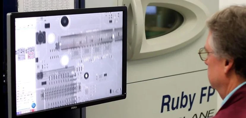
For customers who do not want to destructively analyze their assemblies, Nextek also offers advanced, non-destructive virtual cross sectioning via the latest generation of 3D x-ray laminography equipment.
DYE AND PRY
A destructive test method utilizing high density penetrant dye to evaluate opens or fractures in solder interconnects.

3D X-RAY LAMINOGRAPHY
Using Nextek’s Ruby Dage 3D X-Ray System, our lab staff can perform virtual cross sectioning on electronic assemblies. This methodology has the inherent advantage of being a non-destructive verification and validation of opens on hidden solder joints.
SCANNING ELECTRON MICROSCOPE (SEM) WITH EDS
Our JEOL Scanning Electron Microscope (SEM) with EDS is the latest generation technology platform used for metallurgical analysis. Low vacuum analysis can be performed on samples allowing for Non-Destructive Analysis and elemental mapping.
IONOGRAPH TO MEASURE PARTICULATE CONTAMINATION ON PCBS AND PCBAs
Contamination at the bare PCB level can lead to catastrophic failures in the field. Our lab staff tests every receipt of PCBs for ionic contamination prior to release for production.
COUNTERFEIT PART MITIGATION
With the increasing number of counterfeit electronic components being introduced into the market, Nektek's counterfeit part mitigation services are extremely important. Any suspect brokerage parts are sent to the analytical lab for verification and validation before they are released to the manufacturing group. Counterfeit part mitigation can catch inferior and non-working components that can lead to major failures in electronic assemblies.